
Professional Chip Resistor Essentials: Selection, Performance and Circuit Design
2026-11-16
Selecting the right chip resistor can make or break your circuit, especially when precision and reliability are non-negotiable. This guide dives into the essentials of chip resistor performance, materials, and design trade-offs—arming you with the criteria to choose components that truly fit your application. Whether you're tackling thermal management or chasing tight tolerances, understanding these fundamentals is key. For the latest precision resistor solutions, visit Milliohm and explore options engineered for demanding analog and mixed-signal designs.
Chip Resistor Types and Their Hidden Quirks
Thick film chip resistors may be the workhorses of the electronics world, but they have a well-kept secret: their resistance can drift noticeably under high humidity or voltage stress due to moisture ingress into the porous glass matrix. This often goes unnoticed until a precision circuit starts misbehaving at the worst possible moment. Thin film types, on the other hand, offer far better stability and lower noise, yet they come with their own quirk—their high sensitivity to mechanical strain. Even the subtle board flex during thermal cycling can shift values enough to confuse sensitive feedback loops if you're not careful with layout.
Metal foil resistors seem like the perfect upgrade until you encounter their hidden inductance in certain trimming patterns, which turns them into tiny antennas at higher frequencies. Meanwhile, current sense resistors built with metal alloy elements can develop microcracks at the termination interfaces after repeated temperature shocks, silently increasing resistance until your efficiency calculations fall apart. The real trap lies in assuming that same-size resistors from different manufacturers handle pulse power the same way; material differences in the resistive element often mean that a standard 0603 can survive momentary overloads one minute and fuse open the next.
Chip resistors with built-in surge tolerance are often mistaken for ordinary components until a transient event reveals their true nature—or lack thereof. Manufacturers wrap these safeguards in nearly identical outlines, so spotting the difference requires a deep dive into datasheets that tend to bury these quirks in footnotes. The biggest quirk of all might be that designers frequently treat chip resistors as commodity parts, yet their unexpected failures have a habit of teaching expensive lessons about the fine print.
Reading Beyond Resistance: Tolerance, TCR, and Power Ratings
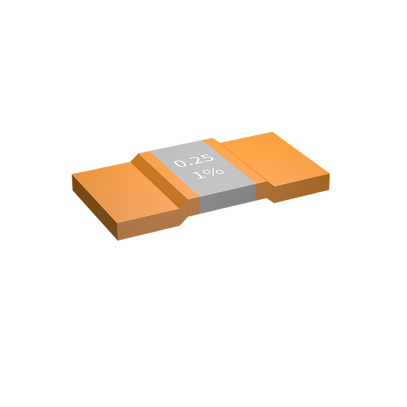
Resistance is rarely a fixed number in real-world circuits. Drift happens—sometimes due to aging, sometimes due to soldering heat, and almost always with temperature swings. That’s where tolerance and TCR (Temperature Coefficient of Resistance) step in. Tolerance tells you the initial spread at room temperature, but TCR reveals how much that value may wander as the component heats up or cools down. Picking a 1% resistor might feel safe, yet if its TCR is a sloppy ±200 ppm/°C, a modest 50°C rise can nudge the resistance out of spec faster than you’d expect.
Power rating is the third piece that often gets misunderstood. It’s not a cap you can brush against without consequence; it’s a thermal limit tied intimately to ambient temperature and board layout. Many designers treat a 0.25W rating as a permission slip to dissipate 0.25W anywhere, but the fine print shows derating starts well below the headline number—sometimes at just 70°C. If the resistor sits next to a hot voltage regulator or lacks copper pour for heat sinking, effective power handling can plummet. That’s when you start burning through margins you didn’t know you’d already spent.
Bringing these three parameters together shifts the conversation from “what value do I need?” to “will this value hold under all conditions?” A precision analog front-end might demand a combination of tight tolerance and sub-50 ppm/°C TCR, while a snubber network cares far more about pulse handling than static accuracy. Reading beyond the ohmic number means connecting these dots: tolerance sets the starting line, TCR predicts the path under thermal load, and the power rating dictates how hot the journey gets before performance degrades.
Noise, Stability, and Voltage Effects in Precision Circuits
Every precision circuit lives with an unwelcome companion: noise. It creeps in through resistor thermal agitation, seeps out of semiconductor junctions, and rides in on supply rails. In high-resolution measurement paths, even microvolt-level disturbances can bury the signal you’re chasing. Managing noise isn’t just about picking a low-noise op amp—it’s a negotiation between bandwidth, impedance levels, and layout geometry. Guard traces, split ground planes, and careful filtering become essential when a circuit’s least significant bit weighs only a handful of nanovolts.
Stability often masquerades as a static specification, yet in precision work it is a dynamic tightrope. A circuit that looks rock-solid on the bench can sing at several megahertz under a reactive load, or drift slowly with a whiff of humidity. Small phase shifts that accumulate across a feedback network turn a precision amplifier into a power oscillator without warning. Compensation tricks like pole-zero pairs, feed-forward capacitors, and bootstrapped guard rings are not arcane—they are everyday survival tools for keeping a 24-bit data path linear and quiet across temperature and time.
Voltage effects in precision circuits go well beyond the headline offset and gain errors. Thermocouple junctions form at every solder joint and connector interface, generating microwaves of temperature-dependent voltage that swamp the signal from a strain gauge or thermopile. Seebeck coefficients of common materials like copper-oxide and tin-lead solder can be surprisingly large, making a single unintended junction the dominant error source. Then there are parasitic piezoelectric effects in ceramic capacitors and stress-induced shifts in molded references. Guarding against these subtle voltage intruders means mastering layout symmetry, selecting benign materials, and sometimes sealing a critical node inside a temperature-stabilized cocoon.
Footprints, Layout, and Thermal Relief in Dense Boards
When working with densely packed circuit boards, every fraction of a millimeter counts. Footprint design becomes an exercise in balance, where pad sizes and spacing must accommodate not just the component leads but also the realities of automated assembly and rework. Pushing pads too close together can invite solder bridging during reflow, while undersizing them risks insufficient mechanical anchoring. Layout engineers often find themselves fine-tuning land patterns to match the specific needs of high-density interconnects, sometimes deviating from generic library recommendations to account for signal integrity and thermal behavior under load.
Thermal relief connections transform from simple copper spokes into a critical tuning element. In planes that double as heat sinks, overly aggressive thermal ties can pump heat away faster than a soldering iron can compensate, resulting in cold joints or tombstoned passives. Conversely, insufficient relief chokes the flow of heat during operation, creating local hotspots that degrade performance. On multilayered boards with buried power and ground planes, the interaction between component placement and thermal relief geometry determines whether a design can be manufactured repeatably without excessive hand touch-up.
The layout process itself hinges on understanding how thermal mass distributes across the board. A row of large connectors, for instance, can steal heat from adjacent small-pitch ICs, demanding a rethinking of copper pours or relief spoke dimensions. By strategically placing thermal ties and balancing copper fills, designers manage to keep soldering profiles consistent across parts with vastly different thermal demands. It is a silent negotiation between electrical, mechanical, and manufacturing constraints, and getting it right means the difference between a board that assembles cleanly and one that fights the technician at every joint.
How Parasitics Shape High-Frequency Resistor Behavior
At low frequencies, a resistor behaves much like the ideal component we learn about in textbooks—a simple opposition to current defined by its resistance value. But push the operating frequency into the megahertz or gigahertz range, and that neat picture falls apart. Hidden parasitic elements, such as lead inductance and stray capacitance, start to dominate the impedance profile. What was once a predictable ohmic device morphs into a complex network where the actual impedance can swing dramatically from the nominal value, often introducing unwanted phase shifts and resonances that derail circuit performance.
These parasitic effects aren't just minor corrections; they redefine the component's behavior entirely. The metal leads or terminations exhibit series inductance that creates a rising impedance with frequency, while the end caps and surrounding structures form tiny capacitors that shunt signal energy to ground. In a typical carbon or metal film resistor, this combination effectively turns the part into a self-resonant circuit at some critical frequency. Beyond that point, the parasitic capacitance dominates, and the impedance actually falls with increasing frequency—completely opposite to what the resistor’s DC rating would suggest. Designers who ignore these realities often find their precision attenuators or matching networks performing erratically when signals edge into RF territory.
Manufacturers employ several structural tricks to minimize these unwanted influences, but parasitics can never be fully eliminated—only pushed to higher frequencies. Wraparound terminations, thin-film geometries, and careful substrate choices all help reduce inductance and stray capacitance. Even the resistor’s physical orientation on a printed circuit board matters, as pad size and ground plane proximity introduce additional parasitics. Understanding this interplay is essential for high-speed digital and microwave applications, where a resistor’s true impedance may bear little resemblance to the color bands printed on its body.
Matching Networks and Real-World Application Pitfalls
When designing a matching network for an RF front-end, the textbook approach often assumes ideal components and perfectly characterized loads. In practice, the impedance you're trying to match drifts with temperature, bias conditions, and even the proximity of your hand to a device. A network that looks flawless on the simulator can become a detuned mess once the enclosure is closed or the antenna flexes slightly. Without accounting for these real-world variances, the carefully tuned return loss curve collapses, and you're left chasing ghosts in the production line.
Component parasitics are the silent killers of many well-intentioned impedance matches. A surface-mount inductor that behaves like a pristine 3.3 nH at low frequencies can turn capacitive before you hit 2 GHz. Capacitors have self-resonance modes that destroy the expected phase response. Even the PCB traces between components introduce series inductance and shunt capacitance that shift the match center frequency. Ignoring these second-order effects leads to networks that perform brilliantly in simulation but require constant re-tuning on the bench—an expensive lesson that turns first-pass success into a myth.
Another often-overlooked trap is the assumption of a single operating point. Modern radios hop between bands, switch power levels, and toggle modulation schemes in microseconds. The matching network that presents the perfect 50-ohm load during small-signal lab tests may behave very differently when the power amplifier is driven into compression. Harmonics reflect back into the active stages, efficiency tanks, and linearity degrades. Designing for a single scalar impedance neglects the dynamic nature of the load, and the resulting system works, but never as well as it should.
FAQ
Start by calculating the worst-case power dissipation under maximum voltage or current conditions. Then apply a derating factor—typically 50% to 70% of the resistor's rated power—to account for ambient temperature rise, reduced airflow, and adjacent hot components. Always check the manufacturer's derating curve, as the rated power often assumes a specific board layout and ambient temperature, usually 70°C, with linear derating to zero at a higher temperature.
High-frequency behavior is dominated by parasitic inductance and capacitance. Thin-film resistors usually outperform thick-film due to lower noise and tighter tolerances, but even more critical is the package size: smaller footprints like 0201 or 0402 minimize parasitic effects. Also consider termination style—flip-chip or wraparound terminations can reduce inductance. Look at the resistor's impedance versus frequency plot if available, and be cautious about using values above a few hundred ohms where parasitics start to dominate.
Resistance shift often comes from solder joint stress or excessive heat during assembly. Thick-film resistors can experience a small permanent change due to the glass frit re-melting and mechanical relaxation. Ensure your reflow profile stays within the resistor's specified peak temperature and time. Also check board pad design: mismatched thermal mass between pads can cause tombstoning or uneven wetting, leading to internal mechanical strain. A short post-solder thermal stabilization anneal can sometimes recover a few tenths of a percent.
For low-cost, low-precision sensing you can, but you'll sacrifice accuracy and temperature stability. Dedicated current-sense resistors use low-resistance alloys with low TCR (temperature coefficient of resistance) and a four-terminal Kelvin connection to eliminate lead resistance errors. A standard thick-film resistor's TCR of ±200 ppm/°C can cause significant measurement drift over temperature. If your accuracy requirement is better than 5% across the operating range, move to a metal-element or metal-strip part.
Thin-film resistors are sputtered with a nickel-chromium alloy, giving a uniform thickness that results in tighter initial tolerance (down to ±0.01%) and a much lower TCR (as low as ±5 ppm/°C). Thick-film resistors are screen-printed from a paste and laser-trimmed, which inherently produces more noise, higher voltage coefficient, and a larger temperature drift, typically limiting them to 0.5% tolerance and ±50 ppm/°C at best. For precision analog circuits or high-stability divider networks, thin-film is the clear winner.
Whiskers are a concern mostly with pure tin finishes, but most chip resistor terminations now use nickel barrier layers with matte tin overcoat. The nickel prevents copper diffusion and suppresses whisker formation. Avoid pure tin-plated parts in high-humidity, high-sulfur atmospheres. For high-reliability applications, specify a tin-lead solder finish or gold terminations. Conformal coating can also reduce tin whisker risk by blocking corrosion pathways.
At high resistance values (typically above 1 MΩ), the effective resistance can drop as voltage increases due to the non-ohmic behavior of the thick-film materials and leakage along the surface. This voltage coefficient of resistance (VCR) is usually expressed in ppm/V. In voltage dividers or feedback networks, a large VCR can introduce nonlinearity in your circuit. If your application spans wide voltage swings, choose a resistor specified for low VCR or use multiple lower-value resistors in series to distribute the voltage.
Conclusion
Beyond the simple ohm value printed on a schematic, every chip resistor brings its own set of hidden behaviors that can make or break a design. Thick-film types, for instance, are economic workhorses but introduce current noise that rises at low frequencies, and their voltage coefficient of resistance can skew readings in high-impedance circuits. Thin-film and metal-foil varieties tame these quirks with tighter tolerance, much lower temperature coefficient of resistance (TCR), and superior long-term stability, yet they demand a careful reading of datasheets because a ±25 ppm/°C TCR spec rarely tells the full story of how resistance drifts across the actual operating temperature range. In precision analog paths, self-heating under load, excess noise, and even subtle voltage-dependent effects accumulate, so rating a part solely by its power number invites trouble. Power derating is never a straight line down to zero; board copper area and ambient airflow reshape the thermal landscape entirely.
Footprint selection ripples through both thermal and high-frequency performance. A tiny 0201 package reduces parasitic inductance and suits dense RF boards, but its minuscule size limits heat dissipation and makes rework a delicate task. Layout choices, such as the amount of copper connected to pads and thermal relief spoke widths, directly influence how much current a resistor can handle before its temperature soars. At gigahertz speeds, the humble chip resistor ceases to behave as a pure resistance; series inductance from terminations and parasitic shunt capacitance create a complex impedance that can shift matching-network behavior, degrading filter response or introducing unexpected resonances. Real-world pitfalls arise when designers treat a matching network as a schematic ideal—board parasitics, component tolerances, and thermal gradients between nearby components can easily detune a carefully calculated network, highlighting why repeated prototyping and environmental testing remain irreplaceable.
Contact Us
Contact Person: Yuying Gao
Email: [email protected]
Tel/WhatsApp: +86 18926013721
Website: https://en.milliohm.net/