
Chips Production Line Factory: Unveiling the Future of Semiconductor Manufacturing
2026-05-25
Step into the heart of modern semiconductor fabrication, where precision meets innovation. The chips production line factory isn't just a facility—it's the engine driving tomorrow's technology. At MINGDE, we're redefining what's possible, merging speed, accuracy, and scalability in ways the industry has never seen. Curious about how a single line can shape everything from AI to autonomous vehicles? You're about to find out.
Inside the Ultra-Clean Production Floors
Step through the airlock and the first thing you notice is how still the atmosphere feels. Every breath is meticulously filtered, every surface engineered to shed nothing. Workers glide in full bunny suits, their movements deliberate and practiced, as if choreographed to avoid disturbing a single particle. This isn't sterility for the sake of sterility—it's the bedrock of yields that make cutting-edge chip fabrication economically viable. A single speck of dust drifting onto a wafer can kill a die that costs thousands of dollars to produce, so here, contamination isn't a nuisance; it's catastrophe in waiting.
The floor plan itself dictates the rhythm of cleanroom life. Materials enter through air showers and pass-through chambers, while personnel spend long minutes gowning up before even glimpsing the production line. Overhead, massive fan filter units hum quietly, driving laminar airflow that pushes particles down and out through grated flooring. It creates a subtle downward current you can almost feel on your skin—a constant reminder that the room is alive, breathing in unison. Monitoring systems track particle counts in real time, adjusting pressure differentials and humidity with a precision that rivals the tools building the chips themselves.
What strikes you most is the quiet. Not the silence of emptiness, but a concentrated hush born from extreme discipline. The tools—lithography steppers, etchers, deposition chambers—sit in solemn rows, their inner vacuums and plasma glows hidden behind panels. Technicians communicate in clipped, efficient phrases, often via headsets. There’s no clutter, no stray cables, no coffee cups. Everything has a place, and every action follows a protocol. It’s an ecosystem engineered to eliminate variables, where human ingenuity focuses entirely on the nano-scale dramas unfolding inside the machines.
How Automation Shapes Every Wafer
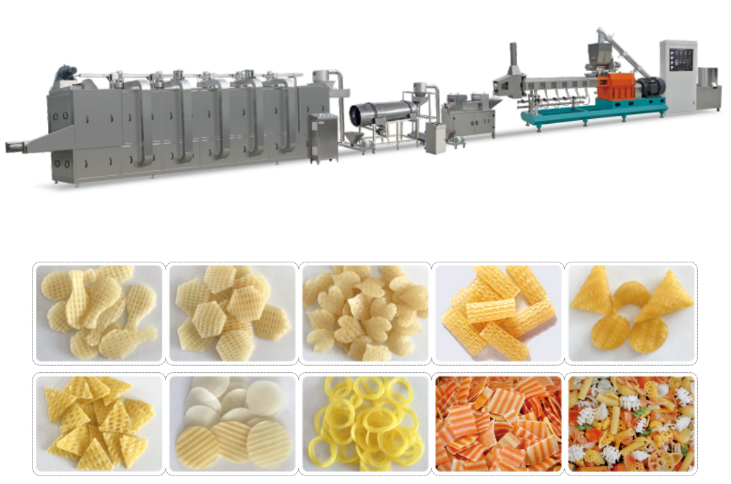
In semiconductor fabrication, each wafer travels through hundreds of intricate steps, where even microscopic inconsistencies can ruin entire batches. Automation steps in as the silent guardian, orchestrating material handling, process control, and inspection with a precision no human operator could sustain. From the moment a bare silicon disc enters the line, robotic arms and conveyor systems take over, shuttling it between photolithography, etching, and deposition tools without introducing contamination or mechanical stress. This level of orchestration ensures that every wafer, regardless of when or where it's processed, receives the exact same treatment.
Beyond mere transport, automation embeds intelligence into the fabrication flow. Sensors constantly monitor temperature, pressure, and chemical concentrations, feeding data to adaptive control loops that make real-time adjustments. If a plasma etch drifts slightly, the system tweaks parameters on the fly, preserving critical dimensions across the entire wafer surface. Such closed-loop control transforms manufacturing from an art into a reproducible science, where the goal isn't just making one perfect wafer—it's making every wafer perfect. Automated defect inspection then validates each layer, flagging anomalies down to nanometer-sized particles, so that nothing slips through unnoticed.
The cumulative impact of automation extends far beyond yield rates. It enables the rapid scaling of production without a proportional increase in human oversight, allowing fabs to churn out millions of identical chips each month. More importantly, it accelerates learning: every data point from automated processes feeds into digital twins and machine-learning models that constantly refine the manufacturing recipe. In this way, automation doesn't just shape individual wafers—it shapes the entire evolution of chipmaking, pushing geometries smaller and performance higher with each iteration.
The Materials Revolution Behind Faster Chips
For decades, silicon has been the undisputed king of chipmaking, but we're now brushing against its physical limits. To keep the pace of performance gains, engineers are turning to exotic materials like gallium nitride and silicon carbide, which can handle higher voltages and switch faster. These compounds are quietly replacing traditional silicon in power amplifiers and 5G infrastructure, slicing energy waste and enabling sleeker, more responsive devices.
At the transistor level, the shift is even more dramatic. The industry is moving away from pure silicon channels toward materials such as indium gallium arsenide and even two-dimensional layers like molybdenum disulfide. These semiconductors offer superior electron mobility, meaning data can zip through with less resistance. It's a delicate dance of material science—each new layer must be just a few atoms thick and flawlessly integrated, which has been a stubborn manufacturing challenge.
Interconnects, the tiny wires that shuttle signals across a chip, are also getting a radical makeover. Copper is hitting its limit at the smallest scales, so researchers are experimenting with cobalt and even exotic solutions like graphene or carbon nanotubes. By reducing resistivity and electromigration, these materials help cram more transistors into a given space without the usual penalties in heat or speed. It's this kind of behind-the-scenes innovation that will keep Moore's Law breathing a little longer.
Precision at Nanometer Scale
Working at the nanometer scale demands an entirely different mindset compared to conventional machining. Here, a single misplaced atom can alter the behavior of a material or device, making consistency and repeatability the real benchmarks of success. It's not just about hitting a target once—it's about doing it thousands of times without drift, across wafers, tips, or molecular assemblies. The tools we rely on, from electron-beam lithography to atomic force microscopes, must be isolated from vibrations that measure in mere fractions of a nanometer. Temperature fluctuations, acoustic noise, even the footsteps of someone walking past the lab can become sources of error that ruin hours of painstaking work.
Achieving this level of precision often involves closed-loop feedback systems that correct positioning in real time. Optical encoders and laser interferometers track stage movements with sub-nanometer resolution, while piezoelectric actuators make adjustments faster than the human eye can perceive. But hardware alone isn't enough—software algorithms model thermal expansion, compensate for non-linear stage behavior, and predict wear on diamond tips or nanoindenters. In fields like semiconductor fabrication, the overlay accuracy between successive layers must stay within a tolerance that now approaches just a few nanometers, a constraint that pushes metrology to its very limits. Every measurement is a negotiation between what we can detect and the inherent noise of the instruments themselves.
The real art lies in striking a balance between resolution and throughput. The most exquisite atomic-scale manipulation is useless if it takes ten hours to pattern a single square millimeter. Researchers constantly tweak exposure doses, resist chemistries, and environmental controls to speed up processes without sacrificing the fidelity of the final structure. This tightrope walk defines modern nanotechnology, where breakthroughs often come not from a single machine but from the quiet, iterative refinement of entire process chains. It's a discipline where patience meets physics, and the smallest adjustments yield the most profound results.
Sustainable Manufacturing for Tomorrow
Manufacturing's next chapter isn't just about efficiency—it's about rethinking how we make things so that both industry and environment can thrive. Tomorrow's factories will run on circular principles, where waste from one process becomes raw material for another, and energy systems are designed to regenerate rather than deplete. This isn't a distant vision; it's already taking shape in pilot lines that use bio-based materials, closed-loop water cycles, and real-time data to slash resource consumption without sacrificing output quality.
The real shift happens when sustainability stops being a compliance checkbox and becomes a design language. Engineers are now embedding lifecycle thinking into product DNA, choosing materials that can be endlessly remanufactured or safely returned to the biosphere. Additive manufacturing plays a quiet but pivotal role here—building components layer by layer eliminates the cut-and-carve waste of traditional methods, while also enabling on-demand production that sidesteps overstock and obsolescence.
Perhaps the most overlooked ingredient is workforce ingenuity. The factories of tomorrow will rely on teams who blend traditional know-how with digital fluency, constantly tweaking processes to find unexpected resource savings. When machine operators and data analysts collaborate on energy mapping or supply chain loops, the results often outpace what top-down initiatives can achieve. It's this human layer of creativity—more than any single technology—that will anchor sustainable manufacturing in the real world, making it resilient, profitable, and genuinely future-proof.
From Silicon to System: The Integration Journey
The transformation from a bare silicon die to a fully functional system is a meticulous orchestration of design, packaging, and validation. It begins at the transistor level, where engineers wrestle with nanoscale physics to balance performance and power. Yet, the real magic happens when these microscopic circuits are woven into a cohesive architecture—interconnects, memory hierarchies, and I/O blocks must converse seamlessly, often across different clock domains and voltage islands. This bridging of the abstract logical design and tangible physical reality is where the true art of integration lies.
Packaging technology has evolved from a simple protective shell into a critical enabler of system performance. Advanced techniques like 2.5D interposers and 3D stacking blur the line between chip and system, allowing heterogeneous dies—processors, memory, and analog components—to be fused into a single entity. This approach sidesteps the limits of monolithic scaling, but it introduces a new universe of challenges: thermal dissipation, signal integrity across microbumps, and the co-design of power delivery networks that must satisfy the voracious appetite of modern workloads. Each layer of the stack demands a collaborative dance between fabrication, assembly, and test engineering.
Validation is the silent gatekeeper of this journey. A system-on-a-package may look flawless on a blueprint, but actual behavior emerges only through exhaustive bring-up and corner-case testing. Firmware, drivers, and application software must be tuned to the silicon’s idiosyncrasies—timing glitches that only surface under specific voltage-temperature corners, or memory controllers that stumble on rare access patterns. The integration journey isn’t complete until the system runs real-world tasks reliably, proving that the intricate web of analog, digital, and software components can truly work in harmony.
FAQ
It integrates cutting-edge lithography, AI-driven defect detection, and fully automated material handling, pushing the boundaries of precision and efficiency far beyond current industry standards.
By employing advanced multi-patterning techniques and real-time process adaptation, it can handle sub-3nm nodes with remarkable yield rates, turning theoretically daunting layouts into manufacturable realities.
The facility uses closed-loop water recycling, energy-efficient lasers, and smart power management to slash consumption per wafer, proving that high-volume output doesn’t have to come at the planet’s expense.
Humans remain essential for oversight and innovation, but the factory floor is heavily automated—autonomous vehicles and robotic arms handle repetitive tasks, freeing engineers to focus on optimization and breakthrough experiments.
Inline metrology and nanoscale imaging systems scan every layer in real time, using machine learning to spot anomalies that even seasoned technicians would miss, ensuring near-perfect dies.
The immense capital investment and the need for a highly specialized supply chain—from ultra-pure chemicals to customized equipment—makes rapid expansion difficult, though modular factory designs are starting to lower the barrier.
Possibly, through shared fab models or cloud-based chip design platforms that hook directly into such advanced lines, letting startups prototype without owning a fab—democratizing access to bleeding-edge silicon.
The ultra-precise positioning systems and contamination control methods could ripple into biotech, quantum computing hardware, or even space manufacturing, where cleanliness and accuracy are equally paramount.
Conclusion
Step onto the production floor of a state-of-the-art chip fabrication plant, and you enter a world where the air is thousands of times cleaner than a hospital operating room. Every surface gleams under amber lighting, designed to protect light-sensitive chemicals. Robotic vehicles glide silently along overhead tracks, ferrying wafer carriers between tools with a precision that eliminates human handling. This is the realm of extreme automation, where each silicon wafer—destined to become hundreds of processors—undergoes over a thousand individual steps without ever being touched by human hands. The machinery operates with a rhythm honed by data, constantly self-adjusting to maintain yields that defy the chaos at atomic scales.
Yet the true marvel lies deeper. Within these tools, materials are engineered at the nanometer level—single atomic layers deposited, etched, and modified to coax electrons through gate-all-around transistors that are mere atoms wide. The shift from traditional silicon channels to exotic compounds like gallium nitride and the introduction of high-numerical-aperture EUV lithography push patterning to limits once deemed impossible. Manufacturers are now integrating chiplets into advanced packages, assembling systems on an interposer as if constructing a microscopic city. And underpinning it all is a sweeping commitment to sustainability: massive recycling systems reclaim water and chemicals, while AI-optimized energy grids slash consumption, proving that the future of computing can be built without mortgaging our planet. From raw sand to packaged system, the journey is an intricate dance of physics, chemistry, and smart engineering—truly unveiling the future of semiconductor manufacturing.
Contact Us
Contact Person: LILY SUN
Email: [email protected]
Tel/WhatsApp: 0086-13969103791
Website: https://www.snackfoodmachinery.com/